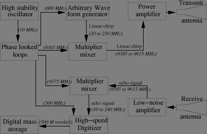
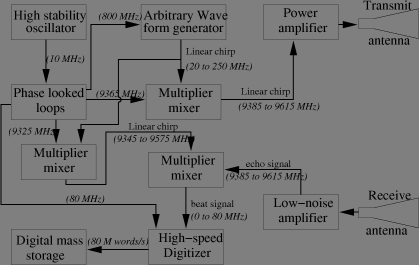
The following global bloc diagram shows the principle of a generic SAR hardware. Though conceptual, the frequency values correspond to our example image (so called X-band or around 9.5 GHz). All signals are derived from an high stability master oscillator. Its high stability is required because of the long integration time involved in the synthetic antenna computation. Current designs include either an atomic clock (Rubidium) or more commonly a cristal oven oscillator (OXO) which is an oscillator with a quartz cristal cast (in fact most often a cristal couple) in such a manner its resonant frequency shows an extremum at a temperature around 60°C. The device being operated inside a casing thermostated at this temperature (the oven).
Why is the hardware so complex? Indeed, it would be possible to have an higher frequency oscillator (say 20 GHz), and dircetly connect the arbitrary waveform generator to the power amplifier. Symetrically, the low-noise amplifier could be directly connected to an higher rate (20 Giga-samples/s) digitizer, and an higher capacity and datarate mass-storage system. Such a simplistic scheme however is only practical for very low frequency operating radars (typically UHF/VHF). For our example image (X-band), it will require 25 times faster and larger memory and digital-to-analog converters in the AWG part, 40 times faster digitizer and 40 times faster and larger mass-storage, for producing the same image. Due to the cost and speed of today memory and storage, this is not interesting (and not even feasible I fear).
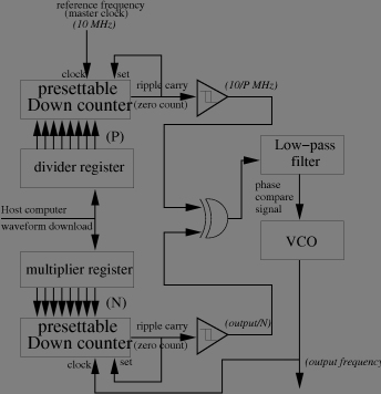
Phase looked loops (PLL) produces coherent multiples of the master clock frequency. In principle, a phase locked loop is a voltage controlled oscillator (VCO) which is controlled by a phase comparison between the reference (master) clock and the divided VCO output(by down-counting the signal periods). Here is the schematics of a PLL, of course, the real design is more complicated, noteworthly for the initial locking hardware. In case the radar frequency is shifted from pulse to pulse (the so called frequency agility technique), there can be either as many PLL's as frequecy steps and a muliplexer, or a fast frequency switching PLL (as a COMSTRON) in which the initial phase looking mechanism is extremely efficient and fast.
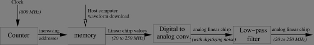
and the arbitrary wave generator (AWG) produces the linear frequency ramp (chirp) needed for pulse synthesis. An AWG is basically a counter addressing a random access memory containing the sampled numerical values of the signal and a digital to analog converter.
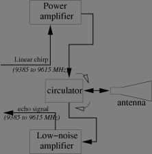
The above main bloc diagram is in the simplest case of a quasi-monostatic radar (in which the transmit and receive antennae are distinct though on the same carrier craft. This is the case of our example image. (indeed there are one transmitting antenna -emitting alternatively in vertical and horizontal polarisation- and two recieve antennae -receiving simultaneously vertical and horizontal polarisations-). This two-antenna design is compulsory in case transmit and receive occur simultaneously (the continuous wave -FMCW- SAR sometimes used for very short range application). There are case where only one antenna can be used both for transmit and receive, generally for weight and space considerations. In these cases, the antenna needs a sort of a switch between transmit and recieve cables. This switch could be a circulator a triode with one input, one output and a bidirectional port, which is commanded by a magnetic field acting on a ferite core. This sort of switch -with no mecanically moving part- can be operated at frequency of a few kHz (typical of the pulse repetition frequency) with radio frequency signals.
Multipliers/mixer blocs involved in the above diagrams are used to add/substract frequencies in order to raise the logic generated signals (output of the AWG) to radiowave frequency and conversely to lower radiowave frequency signals to frequency accessible to digitisers. There are in fact only assymetrical phase multipliers. Namely, given a strong command signal, and a small measured signal, they change the sign of the measured signal when the command signal is negative, and leave it unchanged if the command signal is positive. In fact, the command signal must be strong because no mesured signal is transmitted at all when the command signal amplitude is below the voltage threshold of the diode bridge. From the identity cos(a) cos(b) = ½cos(a+b) + ½cos(a-b) we can see that signals with the sum and the difference of command and measure signals are generated, one of which can be selected by a band-pass filter:
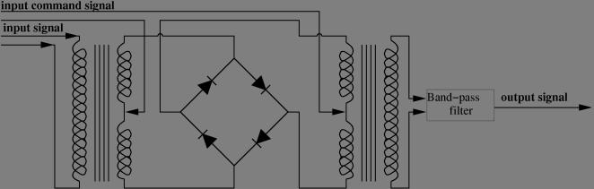
In practice, the frequency increases and decreases are made by two successive frequency mixing because the AWG bandwidth (+20 to +250 MHz in our example) is very near from its mirror frequency band (-250 to -20 MHz), thus after a single step mixing, the band-pass filter should suppress efficiently the of the «frequency sum» band (9115 to 9345 MHz in our example) while leaving unaltered the «frequency difference» band (9385 to 9615 MHz) which is very close to it.
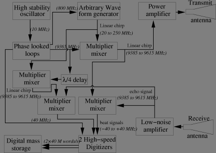
The global bloc diagram at the top of this page correspond to a generic radar in which the pulse synthesis is fully digital (i.e. done in the signal processing computer). Note that this requires a sampling frequency of at least twice the emitted chirp bandwidth (in our example 500 Msamples/s for a 230 MHz bandwidth). Part of the range processing can be done with the hardware by instead of multiplying the received signal by a constant frequency, multiplying it by (part of) the initial linear frequency ramp -called the replica-. This results in a lower bandwidth signal (hence lower sampling frequency and mass-storage requirements) to the cost of a limited swath (interval between the nearest and the farest imaged range). Mathematical details of this technique will be discussed later, but the hardware look like this:
The main problem with deramp radar design, is that the output low-pass filter of the last multiplier need to be sharp edged (otherwise the terrain out of the imaged swath get wrapped on the visible swath, producing smearings). Because of its sharp edges, it introduces amplitude and most severely phase distorsions that may be very annoying for certain applications (most notably the interferometric of the fine polarimetric calibrations). These defects can be -at least partially- removed by the signal processing done afterwards.
The above design produced real data (i.e. single channel). It is possible to reduce to the half the sampling rate, by duplicating the receiving channels (thus the datarate remains identical). The channels correspond to demodulation by two signals separated by a quarter of wave (similarly to cosinus and sinus functions). The first channel is denoted I, or real part or phase channel, while the second is denoted Q, or imaginary part or quadrature channel. The idea behind this is that the Niquist criterium (minimum sampling rate) is once the bandwidth for complex-valued signals while it is twice the bandwidth for real-valued signals (because the spectrum of a real-valued signal is even, it is not possible to discriminate positive and negative frequencies). The corresponding hardware (in the deramp case) look like this:
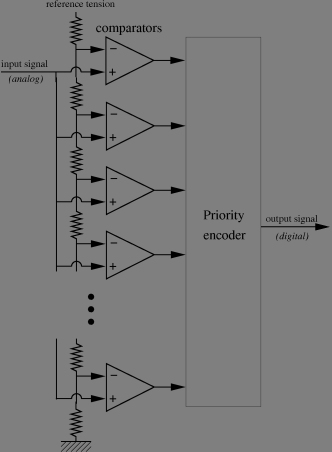
Fast digitisers are made of a bank of finely tuned (laser adjusted) resistors providing a set of evenly spaced tensions. Each tension is compared with the signal to be digitized (sampled-and-hold and tension shifted) with an saturated operational amplifier (thus acting as a comparator). The outputs of the comparator (255 of them in case of an 8-bit digitiser) are encoded with a logic gate circuit called priority encoder, which provides the binary address of its first non-zero input.